Chopper-Stabilized Amplifiers With a Track-and-Hold Signal Demodulator
Abstract—The conventional signal demodulator of a chopper amplifier can be substituted by track-and-hold (T/H) and averaging functions. This arrangement provides offset cancellation without requiring low-pass filters and can ignore the residual offset generated by input spikes. A noise analysis shows that this T/H demodulator degrades the white noise signal-to-noise ratio (SNR), although degradation can be minimized by using maximum duty cycle and minimum amplifier bandwidth.
Index Terms—Broadband white noise semiconductor, chopper amplifiers, offset cancellation, track and hold demodulator.
I. INTRODUCTION
The chopper stabilization of amplifiers is a well-known technique for reducing the input direct current (DC) offset and low-frequency input noise that usually degrades the performance of precision DC amplifiers [1]−[3]. Fig. 1 shows the basic principle.
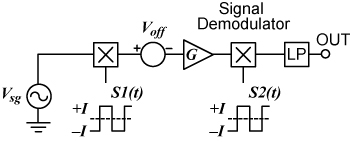
Fig. 1. Conventional chopper-stabilized amplifier.
The input signal is first multiplied by a unit symmetrical square wave function S1(t) of frequency ƒclk , then amplified by an amplifier of gain G, multiplied again by a switching function S2(t) similar to S1(t), and finally low-pass filtered. The first multiplication translates the input signal spectrum into the high-frequency (HF) region and the second recovers the amplified original signal by demodulating the signal back to the base band. On the other hand the input-referred amplifier DC offset and low-frequency noise components go only through the second multiplication process. The DC offset, for example, being converted into an HF square wave function that is fully attenuated by the low-pass filter. The multiplication functions are usually implemented by simple pairs of metal-oxide-semiconductor (MOS) switches controlled by the CLK signal.
A problem of the conventional chopper lies in the possible generation of parasitic offsets due to the first multiplication switching transients, these offsets going through the low-pass filter uncancelled. Another problem is the low-pass filtering required for attenuating the residual square wave ripple due to the offset. This is particularly severe in monolithic choppers where multiplepole LP filters require an appreciable silicon area.
We describe next the pros and cons of replacing the conventional signal demodulator by a track-and-hold (T/H)-based demodulator.
II. THE TRACK-AND-HOLD SIGNAL DEMODULATOR
Let us assume that the input signal to the chopper-stabilized amplifier Vsg is bandwidth limited to the Nyquist frequency (ƒclk ⁄ 2) and that the amplifier is noiseless.
The residual offset due to input switching transient spikes which are short as compared to Tclk ⁄ 2 can be reduced appreciably by narrowbanding the amplifier as much as possible [2] or including a bandpass (BP) filter with center frequency locked to ƒclk [4]. In cases where the chopper operates at relatively higher frequencies and the input spikes duration is no longer negligible as compared to Tclk ⁄ 2, similar results can be achieved by widebanding the amplifier and making S2(t) a switching function with a lower than 50% duty cycle, as shown in Fig. 2, such that during Δt intervals, where the amplified spikes lie, the output is zero. This technique introduces a signal attenuation given by Δt ⁄ (Tclk ⁄ 2) and a larger white noise.
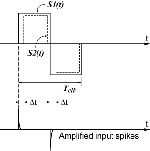
Fig. 2. Input spike removal by proper shaping of the second multiplier switching function.
The signal attenuation can be avoided and the low-pass filter requirements relaxed when a holding function is appropriately included in the signal demodulator. For example, Fig. 3 shows a signal demodulator comprising a two-T/H plus an adder (or averaging) arrangement that could be used instead of the conventional signal demodulator of Fig. 1.
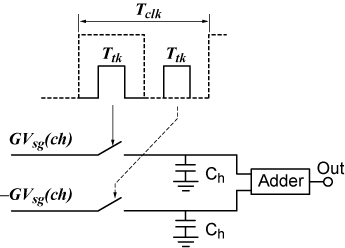
Fig. 3. T/H demodulator.
The T/H inputs are the noninverted and inverted amplified chopped signals, while the T/H outputs are applied to the adder. The T/H switches are closed by pulses occurring during the CLK and the CLK_bar timing signals with duty cycle d. We assume that the chopped signal goes through the amplifier without distortion, which means amplifier bandwidths five or more times the ƒclk.
With this arrangement, assuming ideal switches and zero offset, and recalling that the shopped signal changes sign at each CLK half cycle, each T/H recovers the original signal G × Vsg and the adder generates a 2G × Vsg output which is updated each CLK half cycle.
As far as the DC offset (or the low frequency noise components) is concerned the offset, being not chopped, does not change sign at each CLK half cycle and therefore the T/H outputs are DC voltages with opposite polarities, the offset being cancelled by the adder.
The advantages of this signal demodulator for a chopper-stabilized amplifier can be summarized as follows.
- The offset is cancelled without requiring any LP filtering. Any residual offset is only due to T/H mismatchings and adder inaccuracies.
- Due to the interlaced sampling, the typical staircase ripple associated to the output waveform has a 2ƒclk fundamental frequency, which simplifies its removal.
- Residual offsets due to input switching transients can be removed, if desired, by proper relative phrasing of the tracking pulses without and attenuation penalty.
A signal conditioner using a chopper amplifier with a T/H signal demodulator for cancelling the relatively large offsets occurring in a switched-Hall magnetic sensor was recently reported [5].
Fig. 4 shows a fully differential chopper using the previously described T/H signal demodulator. Switches SWi driven by a square-wave 5-V clock signal CLK1 perform the first multiplication, while switches SW1 and SW2, driven by sampling pulses CLK2 and CLK3 together with C1 and C2 and averaging resistors R1 and R2, make up the T/H signal demodulator. A similar T/H demodulator, fed from the amplifier output but with reverse polarity, has been included in order to generate a fully differential output. The T/H switches are complementary MOS (CMOS) pass transistors, while the input switches are simple N-channel pass transistors in order to intentionally enhance the amplitude of the input transient spikes. The amplifier, with a gain of 40× and a 3-dB bandwidth of 3 MHz, is assumed ideal, its offset being simulated with an input DC generator Voff. Fig. 4 also shows the CLK waveforms, the sampling pulses CLK2 and CLK3 occurring approximately at the center of the CLK1 half cycles.
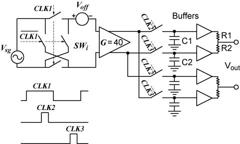
Fig. 4. Fully differential chopper using a T/H signal demodulator.
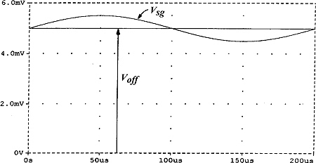
A SPICE simulation of the circuit of Fig. 4 was performed for ƒclk = 160 kHz, d = Ttk ⁄ Tclk = 0.25, a 5-kHz sinusoidal input signal of 0.5-mV amplitude, and a DC input offset of 5 mV. The SPICE model parameters for all devices were derived from a standard 2-µ mixed bipolar CMOS (BiCMOS) process.
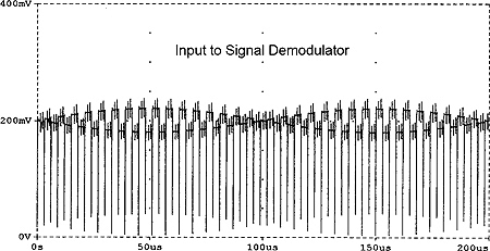
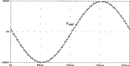
Fig. 5(a) shows the input signal plus the amplifier DC offset waveforms and Fig. 5(b) the voltage waveform at the amplifier output prior to the T/H demodulator. Although the chopped signal appears embedded in relatively large transient pulses, the appropriate relative phasing of the sampling pulses allows clean recovering of the original signal waveform, as shown in the output voltage waveform of Fig. 5(c).
(a)
(b)
(c)
Fig. 5. SPICE simulation of the chopper of Fig. 4. (a) Input signal and input DC offset. (b) Amplifier output voltage waveform, prior to the T/H demodulator. (c) Output voltage.
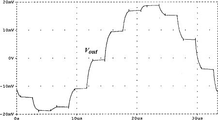
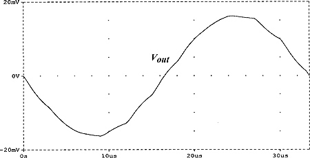
The output voltage is an amplified replica of the input signal except for the quasi-staircase ripple typical of the sample and hold (S/H) functions. As in all sample-data systems, as the signal frequency approaches the Nyquist frequency ƒclk ⁄ 2, the residual staircase ripple becomes more relevant and a postchopper LP filter may be required for recovering the undistorted waveform. For example, Fig. 6(a) shows the same output waveform as in Fig. 5(c), but with the chopper operating at a signal frequency of 30 kHz, i.e., at ≈ 0.4(ƒclk ⁄ 2) the output waveform appearing severely distorted due to the excessive staircase ripple. Fig. 6(b) shows how the original waveform can be approximately recovered by using a postchopper one-pole LP filter with a −3-dB frequency of 60 kHz.
(a)
(b)
Fig. 6. Output waveforms similar to Fig. 5(c) but with the chopper amplifier of Fig. 4 operating with ƒsg = 30 kHz. (a) Without any LP filtering. (b) With a postchopper one-pole LP filter with a −3-dB frequency of 60 kHz.
III. INPUT-REFERRED OFFSET
In the real circuit, the offset cancellation is mainly limited by mismatchings in the demodulator. If Voia is the amplifier input-referred offset, any relative mismatch M = ΔR ⁄ R between resistors R1 and R2 in the adder of Fig. 4 will generate an input-referred offset M × Voia in the chopper, while an equivalent offset Vob due to T/H's and buffer imbalances will generate an input-referred offset Vob ⁄ G. Assuming the residual offset due to input spikes has been removed, and that all imbalances and offsets are statistically independent random function with Gaussian distribution and zero-mean value, we can write for the chopper input-referred offset Voich
(1)
where σ(x) is the standard deviation of x and G the amplifier gain.
Expression (1) shows that, depending on the demodulator imbalances and the amplifier input-referred offset, there is not much to be gained by increasing excessively the amplifier gain.
As in conventional choppers, asymmetries in the amplifier DC transfer characteristics can also limit the offset cancellation by introducing differences between the noninverted and inverted amplified chopped signals. Generally, the use of well-matched differential amplifiers makes this source of error negligible as compared to those given in (1).
Besides, the addition of holding functions and the use of an amplifier with a bandwidth much larger than the clock frequency, degrades the signal-to-noise ratio (SNR) of this type of demodulator, as will be shown in the next section.
IV. NOISE CONSIDERATIONS
In all practical cases, a white-noise voltage, due to the amplifier input-referred white-noise voltage, amplified G times and limited by the amplifier bandwidth, appears at the input of each S/H in the demodulator of Fig. 2.
Let us first analyze the white-noise behavior in one simple T/H. Assume a white-noise voltage with an ideal rectangular noise spectrum of bandwidth BWn and power spectrum density ηi is applied to the input of a T/H and call ηo the noise power spectrum density at the T/H output. As was previously mentioned for avoiding distortion of chopped signals, the amplifier bandwidth must be much larger than ƒclk , therefore BWn » ƒclk and the noise is undersampled by the T/H switch.
The noise generated by the tracking pulses of length d × Tclk do not increase appreciably the output noise, but during the hold time (1 − d)Tclk additional noise is introduced due to fold over of all high-frequency (HF) noise components modulated around the clock frequency harmonics into the base band, making ηo > ηi. This aliasing occurs because the periodic hold behaves as an equivalent ideal S/H function where appreciable aliasing occurs whenever the input spectrum extends over the Nyquist band [6]−[8].
The white-noise transfer function of an ideal T/H has been analyzed by Fischer [6], assuming that the output noise power spectral density is the sum of the noise power generated during the track interval, plus the noise power generated during the hold interval. Focusing our interest on the range 0 < ƒ < ƒclk ⁄ 2 and recalling expressions A2, B5a and B5b of [6] we can write a general expression for the noise power spectral density transfer function of a simple T/H, as follows:

(2)
where the first and second terms represent the track and hold contributions, respectively, ηi and ηo are the input and output noise spectral power densities and
d duty cycle (Ttk ⁄ Tclk);
ƒclk 1 ⁄ Tclk = clock frequency;
h closest integer to the BWn ⁄ ƒclk ratio;
sinc(x) [sin(π × x) ] ⁄ π × x.
Note that for d = 0 there is a pure S/H function with ηo ⁄ ηi = (1 + 2 × h) × sinc²(ƒ ⁄ ƒclk) while for d = 1 there is no S/H, the tracking switch being permanently ON with ηo ⁄ ηi = 1. When parameter h is zero there is no aliasing as the noise input spectrum remains below ƒclk ⁄ 2. When h = 1, 2, 3, etc., there is additional noise due to the input noise spectrum going beyond ƒclk ⁄ 2 reaching the first, second, third, etc., CLK harmonics and folding back into the Nyquist band. As the output noise spectrum is approximately flat within the Nyquist band, (2) can be simplified assuming the worst case of a constant power spectral density equal to the maximum value occurring at ƒ = 0. Thus

(3)
Expression (3), giving the white noise degradation in the Nyquist band for a simple T/H function, has been plotted in Fig. 7 in the range 0 < d < 1 and for various values of h. As expected, the noise degradation is maximum for d = 0 and increases with increasing h.
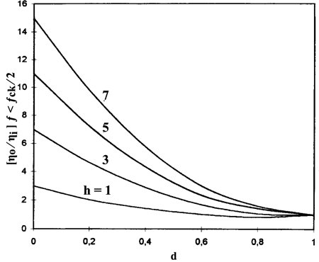
Fig. 7. White-noise power spectral density transfer function of a simple T/H for ƒ < ƒclk ⁄ 2, where d is the track pulse duty cycle and h the closest integer to BWn ⁄ ƒclk, and where the worst case occurring at ƒ = 0 was assumed.
Going back to the demodulator of Fig. 3, the noise outputs of the two T/H's, each one fed by the same noise voltage but with inverted polarities, are added. For the low-frequency region of the noise input spectrum involving frequencies much smaller than ƒclk, the T/H output noise voltages are correlated and therefore cancel out. This cancellation action includes the DC offset voltage and the relatively low-frequency 1 ⁄ ƒ noise. For the rest of the input noise spectrum up to BWn, where most of the noise voltages become uncorrelated and their power spectral densities are directly summed up by the adder.
Thus, with the initial assumption BWn » ƒclk we can assume that practically all the white-noise voltages generated at the two T/H outputs are due to aliasing and therefore uncorrelated; the demodulator of Fig. 3 showing a worst case output noise power spectral density ≈ 2ηo. As the output signal power is four times the input signal power, the demodulator noise figure (NF), as far as the white noise is concerned, becomes
(4)
where η o⁄ ηi refers to the noise power spectrum density transfer function of a single T/H for ƒ < ƒclk ⁄ 2 (Fig. 7).
For example, for d = 0.3 and h = 5, the η o⁄ ηi ratio from Fig. 7 is six and the noise figure of the signal demodulator three. As the tracking pulse width cannot be higher than one clock half cycle, the maximum allowable duty cycle is 0.5 and Fig. 7 shows that the noise due to aliasing is the dominant contributor to the T/H demodulator noise.
V. CONCLUSION
The performance of a chopper-stabilized amplifier where the signal demodulation or second multiplication function is performed by a double T/H and adder arrangement has been described. The most important advantage of this approach, as compared to the conventional chopper, consists in the cancellation of the amplifier input offset, low-frequency input noise components, and residual offsets due to input switching spikes, without requiring any low-pass filtering. The maximum offset cancellation achievable is limited by the T/H mismatchings and by the adder accuracy.
For avoiding excessive staircase ripple on the output waveform, the input signal spectrum bandwidth should be preferably smaller than 0.2 times the Nyquist frequency. Otherwise a postchopper LP filter may be required.
Finally, these demodulators show a white-noise degradation due to the hold function; this degradation being minimum for the maximum allowable duty cycle of 0.5 and minimum amplifier bandwidth.
ACKNOWLEGMENT
The authors would like to thank D. Barrettino, of Electrónica Bilotti, for his helpful suggestions.
REFERENCES
[1] K. Hsieh et al., "A low-noise chopper stabilized differential switched-capacitor filtering technique," IEEE J. Solid-State Circuits, vol. SC-16, no. 6, pp. 708-715, Dec. 1981.
[2] C. C. Enz et al., "A CMOS chopper amplifier," IEEE J. Solid-State Circuits, vol. SC-22, pp. 335-341, June 1987.
[3] C. C. Enz and G. C. Temes, "Circuit techniques for reducing the effects of op-amp imperfections: Autozeroing, correlated double sampling, and chopper stabilization," Proc. IEEE, vol. 84, pp. 1584-1613, Nov. 1996.
[4] C. Menolfi and Q. Huang, "A low-noise CMOS instrumentation amplifier for thermoelectric infrared detectors," IEEE J. Solid-State Circuits, vol. 32, pp. 968-976, July 1997.
[5] A. Bilotti et al., "Monolithic magnetic hall sensor using dynamic quadrature offset cancellation," IEEE J. Solid-State Circuits, vol. 32, pp. 829-836, June 1997.
[6] J. S. Fischer, "Noise sources and calculation techniques for switched capacitor filters," IEEE J. Solid-State Circuits, vol. SC-17, pp. 742-752, Aug. 1982.
[7] C. Gobet, "Spectral distribution of a sampled first order lowpass filtered white noise," Electron. Lett., vol. 17, no. 19, pp. 720-721, Sept. 1981.
[8] C. Gobet and A. Knob, "Noise analysis of switched capacitor networks," IEEE Trans. Circuits Syst., vol. CAS-30, pp. 37-43, Jan. 1983.
Manuscript received November 10, 1997; revised May 2, 1998. This work was supported by Allegro™ MicroSystems, LLC. This paper was recommended by Associate Editor M. Biey.
A. Bilotti is with Electrónica Bilotti, Olivos 1636, Argentina.
G. Monreal is with Sensor Development Group, Allegro MicroSystems, LLC, Concord, NH 03306 USA.
Publisher Item Identifier S 1057-7122(99)02748-8.
The signal demodulator described here is incorporated into the A3150, A3210, A3240, A3260, A3280, A3361, and A3515 Hall-effect sensor ICs. This paper was originally published in the IEEE Transactions on Circuits and Systems, I: Fundamental Theory and Applications, Vol. 46, No. 4, April 1999. Reprinted by permission.
1057-7122/99$10.00 © 1999, IEEE