Using Allegro Current Sensor ICs in Current Divider Configurations for Extended Measurement Range
By Richard Dickinson and Andreas Friedrich, Allegro MicroSystems, LLC
Abstract
Allegro™ current sensor ICs are characterized by innovative packaging technologies that integrate a low-resistance copper primary current conduction path into the package. While this enhances the performance of the application in many ways, there are current level limitations imposed by packaging considerations.
This application note describes simple methods for increasing the measurable current range. These methods involve splitting the path of the current being sensed. Various options of devices and circuits are described.
Introduction
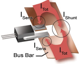
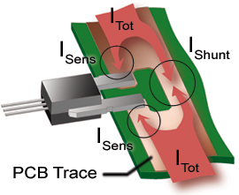
The central element of all Allegro current sensor ICs is a precision linear Hall-effect—based magnetic field sensing circuit. For standard models, the circuit is bidirectional, as shown in figure 1, allowing current flow in either direction.
(A) Higher Current Applications
(B) Lower Current Applications
Figure 1. Current Divider Configurations. The Allegro package primary conductor terminals can be connected directly to a bus bar for higher-current applications. Panel A shows this configuration, with the ACS75x-PSS package option used. For lower current applications, the package can be connected to printed circuit board traces. Panel B shows this configuration, using the ACS75x-PSS package option. For standard models, current can be passed in either direction.
The magnetic field generated by the current is sensed by the integrated Hall IC and converted into a proportional voltage.
Device accuracy is optimized through the close proximity of the current path to the Hall transducer. The integration of the primary current conductor into the package allows extremely well-controlled positioning of the Hall chip relative to the current path. However, the amount of current, IPrimary, that can be routed through the package is eventually limited by physical and thermal considerations.
For measurement of current levels, ITot, that are larger than the maximum of IPrimary, an elegant way of overcoming these limitations is to measure only a well-controlled fraction of the total current, by physically splitting the current path. As illustrated in figure 1, this concept can be applied in higher-current applications by notching a bus bar, and in lower-current applications by using separate branches of PCB (printed circuit board) traces or layers.
There is a disadvantage of this approach. It reduces the current resolution of the system by the same proportion as the current is divided. An optimum solution to compensate can be determined for the proportions of the separate current subpaths. Note that calibration should be done in situ, with the device already assembled to the PCB, in order to take into account any additional resistance in the solder joints themselves.
Sensing a Portion of Current by Using the ACS712 Current Sensor IC
A reference PCB was designed by Allegro that routes one third of the applied current through the ACS712 device. As shown in figure 2, the conduction path on the PCB is a trace that splits the current into two separate subpaths: the shunt current subpath, with a 3.0 mm trace width, and the sense current subpath, with a 5.0 mm width. Figure 3 shows a simulated mapping of the resulting current densities.
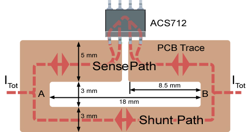
Figure 2. ACS712 PCB Trace Configurations for 1/3 ITot Measurement. The ACS712 is mounted to the PCB trace, in series along the current sense subpath (corresponding to IPrimary through the device).
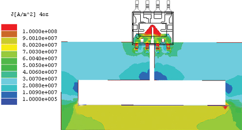
Figure 3. Simulated Current Density for 1/3 ITot Measurement. Data taken at 45 A ITot, with 4-oz. copper trace.
When the reference PCB is fabricated with 4-oz. copper traces, the resistance from point A to point B measures less than 1 mΩ, and the power dissipation less than 2 W. Table 1 compares the calculated resistance and power dissipation for reference PCBs fabricated with 4-oz. traces and with 2-oz. traces.
|
Table 1. Calculated Effect of PCB Trace Weight on Power Dissipation |
||
|---|---|---|
|
Trace Weight |
Power Dissipation at 45 A |
Overall Resistance |
|
4 |
1.14 |
0.56 |
|
2 |
1.94 |
0.96 |
Manufacturing and assembly tolerances result in some small variability in the division of current between the sense subpath and the shunt subpath on individual PCBs. In applications where accuracy requirements make it necessary to compensate for these variations, a customer-programmable version of the ACS712 may be used. This allows the mV/A sensitivity of the IC to be calibrated after board fabrication and assembly.
This incremental improvement in system accuracy, however, must be balanced against the potential of a small percentage yield loss in the ICs, which can result if some of the ICs do not program properly at the customer site. Programming after shipment necessarily means that the devices cannot be 100% final tested at the Allegro factory.
The trace layout dimensions for dividing a current path to measure a given fraction of the total current can be calculated using the equations below (reference figure 4).
Given:
- ISens, measured proportion of ITot (A)
- LSens1, length of sense subpath side 1 (m)
- LSens2, length of sense subpath side 2 (m)
- LShunt, length of shunt subpath (m)
- Ρc, resistivity (typical) of the copper trace material (Ω×m)
- RPrimary, resistance (typical) of the primary conductance path in the device ( Ω )
- T, thickness (typical) of traces (m)
- WSens, width of sense traces (both sides) (m)
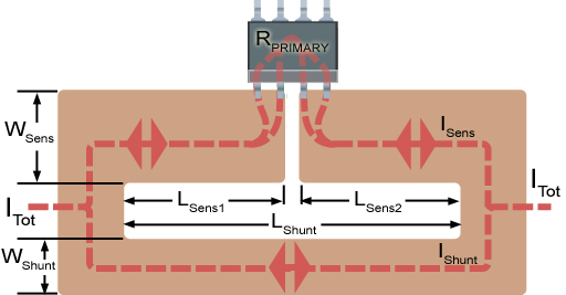
Figure 4. Symbols for Trace Dimension Calculations
The ratio of the resistance of the sense current subpath, RSens ( Ω ), and the shunt current path, RShunt ( Ω ), is defined by the equation for a current divider circuit:
![]() (1)
(1)
where
![]() (2)
(2)
and
![]() (3)
(3)
When calculating the resistance in the sense path, it is important to include RPrimary, the resistance of the primary current conductor, the leadframe, in the ACS712.
For a given ratio of sense current, ISens, to total current, ITot, and a given sense path width, WSens, the required proportions of the trace dimensions can be calculated for the shunt trace path width, WShunt, as follows:
 (4)
(4)
Given, for the reference PCB:
- ISens= ITot / 3
- LSens1= 8.5 mm
- LSens2= 8.5 mm
- LShunt= 18 mm
- Ρc = 2.5 × 10⁻⁵ Ω × mm
- RPrimary= 1.5 m
- T = 0.14 mm; 4-oz. copper
- WSens= 5 mm
then

Equally Splitting Current with Enhanced Resolution
A disadvantage of divider configurations is that they reduce the resolution of the current sensing system. Using two ACS712 devices in parallel, and level-shifting and adding their outputs, reduces this loss of resolution. A sample configuration is shown in figure 5.
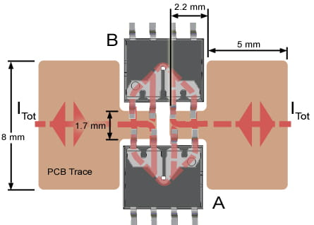
Figure 5. Dual Package Solution Without Reduced Resolution. Divides ITot using two active ACS712 packages.
The schematic diagram in figure 6 shows a circuit to compress the output range of the individual device outputs, and then sum them together. Before output, the signals from each ACS712 are first processed through a subtractor subcircuit with a gain of 0.5. This subcircuit removes the typical 2.5 V offset voltage from the ACS712 output signals.
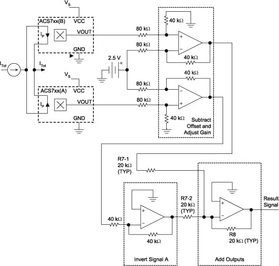
Figure 6. Suggested Circuit for Combining Outputs. This circuit uses two ACS7xx devices to implement an equally divided current path with enhanced resolution.
When oriented as shown in figure 5, device A and device B have opposite polarities relative to the direction of current flow. One of the device outputs must be inverted. By inverting the output of device A, and then using an inverting op-amp for the final addition stage, the overall output signal has the correct polarity.
With unity gain in the final stage, the result is an output signal that has a proportion of ≈ 50 mV per ampere through the parallel ICs, yielding a 0 to 30 A measurement range. A simulation of this is shown in figure 7, and a test trace appears in figure 8.
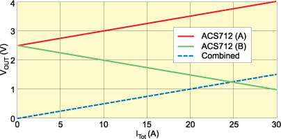
Figure 7. Simulation of Output. Results using ACS712 devices in suggested circuit for combining outputs (figure 6).
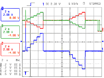
Figure 8. Application of ±30 A Pattern to IPrimary in 6 A Increments. Device A is the green trace, device B is the red trace.The lowest (blue) trace is the output of the interface circuit for combining the two ACS712 outputs. Note that the signals are DC-offset shifted on the oscilloscope, for clarity of viewing.
The resolution will vary with the degree to which the contributions of noise are superimposed onto each other from the two active devices. However, it has been empirically measured that the resulting signal-to-noise ratio is approximately 1.5 times that realized when using a single ACS712 with an uninterrupted current shunt path. If a larger output signal range is desired, the gain may be adjusted by varying the resistor value ratio R8 / R7.
Measuring Currents Higher than 200 A by Using the ACS758 in a Current Divider
As with the ACS712, the measurement range of the ACS758 is limited by the amount of current that can pass through its integrated primary current conductor, which has a resistance of 100 μΩ. In addition, the saturation point of its magnetic concentrator must be taken into consideration.
Figure 9 shows a configuration for a split current path that evenly divides 300 A between the shunt subpath and a sense subpath that contains an ACS758. The resistance across the current divider from point A to point B is calculated as less than 100 μΩ using a 1-mm—thick copper bus bar.
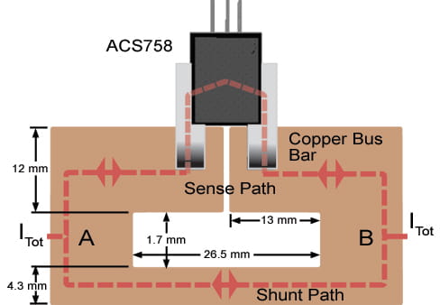
Figure 9. Higher Current Solution. Equally divides ITot using an ACS758 device in series on a 1-mm-thick copper bus bar.
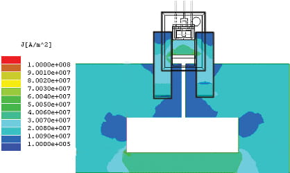
Figure 10. Simulated Current Density for 1/2 ITot Measurement. Data taken at 300 A ITot, with 4-oz. copper trace.
Using multilayer heavy weight PCB traces is an option for additional reduction of power dissipated in a split-current—path assembly. The multiple layers of the PCB allow further division of the current. The ratio of layers allocated to the shunt current subpath to the layers for the sense current subpath determines the total division of the current. Such a configuration is shown in figure 11, which provides both plan and cross-sectional views of a PCB of this type.
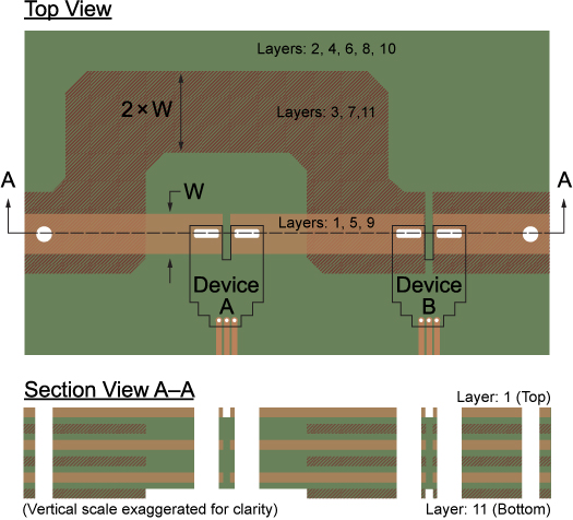
Figure 11. Top and Cross-Section Views of Multilayer Board. This approach, using the ACS758 PFF package option, divides the current according to layer characteristics, passing a controlled proportion of ITot through device A.
In order to adjust for some variability in the current division, a customer-programmable version of the ACS758 may be used. This allows programming the device sensitivity after fabrication of the PCB assembly.
Measuring Currents up to 300 A with Enhanced Resolution Using the ACS758
To enhance resolution in measurements of total currents higher than 200 A, two ACS758 devices can be used in parallel to precisely divide the current. The outputs are level-shifted and added together. This configuration is shown in figure 12. It can be considered for measuring up to 300 A ITot. In order to match a full scale of 300 A, Allegro recommends that the ACS758xCB-150 be used.
The outputs from each ACS758 are first processed through a subtractor subcircuit with a gain of 0.5. This subcircuit removes the typical 2.5 V offset voltage from the ACS758 outputs. The circuit to compress the output range of the individual output signals and sum them is identical to that shown in the schematic drawing in figure 6.
When oriented as shown in figure 12, device A and device B have opposite polarities relative to the direction of current flow. One of the device outputs must be inverted. By inverting the output of device A, and then using an inverting op-amp for the final addition stage, the overall output signal has the correct polarity.
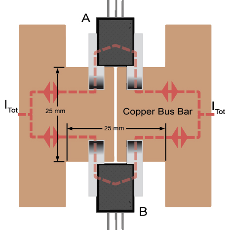
Figure 12. Higher Current Solution. Equally divides ITot using an ACS758 device in series.
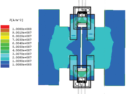
Figure 13. Simulated Current Density for 1/2 ITot Measurement. Data taken at 300 A ITOT, with 4-oz. copper trace.
With unity gain in the final stage, the result is an output signal that has a proportion of ≈ 6.67 mV per ampere through the parallel devices, yielding a 0 to ±300 A measurement range. A simulation of this is shown in figure 14.
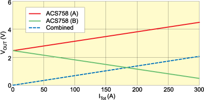
Figure 14. Simulation of Output. Results using ACS758xCB-150 devices in suggested circuit for combining outputs (figure 6).
The resulting signal-to-noise ratio is almost 1.5 times that realized when using a single ACS758 with an uninterrupted current shunt path. If a larger output signal range is desired, the gain may be adjusted by varying the resistor value ratio R8 / R7.
Although the ACS758xCB-150 was used in this case study, by using dual ACS758-200 devices, up to 400 A may be measured with this same configuration and interface circuit. In all configurations, careful attention must be paid to safely matching the bus bar size and heat sinking capacity with the operating current levels.
Conclusion
Through careful board design of split current paths, and by programming device sensitivity after assembly if needed, the Allegro ACS7xx family of devices can be used to measure extended current ranges. For further assistance with a split current path design, please contact your local Allegro sales office and consult with a field applications engineer.
Visit the Allegro Web site for more information on the current sensor IC product lines: