ACS722: High Accuracy, Galvanically Isolated Current Sensor IC

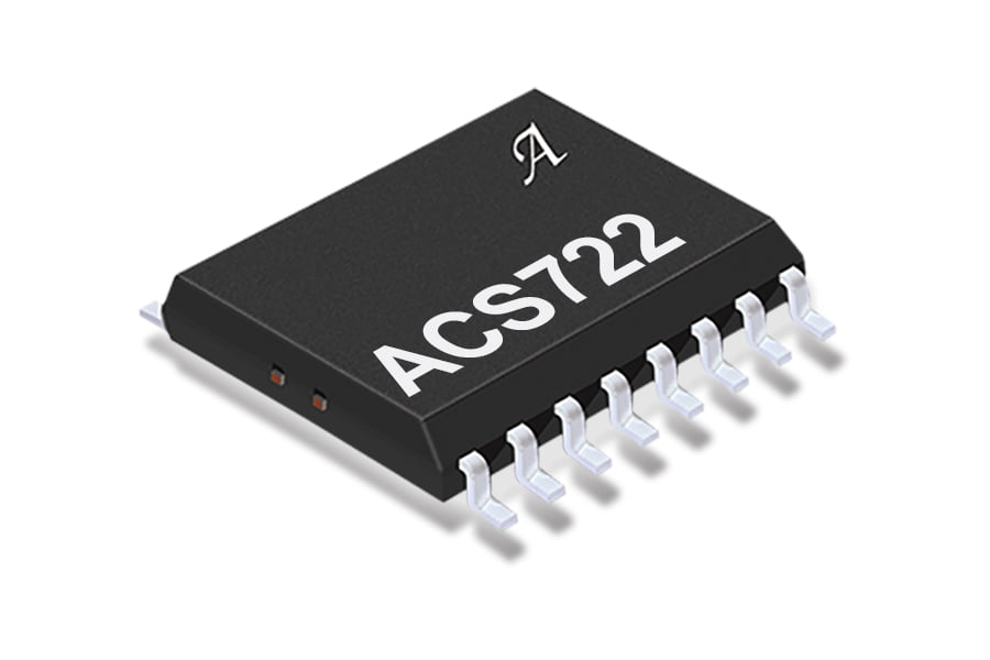
ACS722KMA Product Image

Description

Top Features

Packaging

The Allegro ACS722 current sensor IC is an economical and precise solution for AC or DC current sensing in industrial, commercial, and communications systems. The small package is ideal for space constrained applications while also saving costs due to reduced board area. Typical applications include motor control, load detection and management, switched-mode power supplies, and overcurrent fault protection.

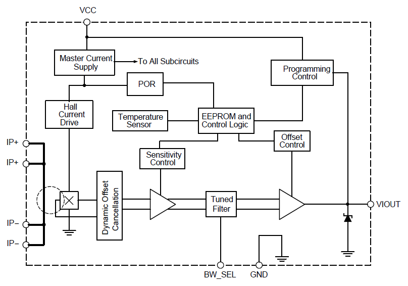
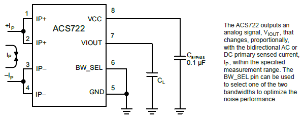
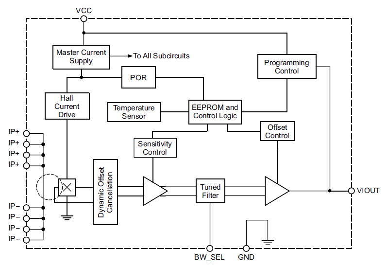
The device consists of a precise, low-offset, linear Hall sensor circuit with a copper conduction path located near the surface of the die. Applied current flowing through this copper conduction path generates a magnetic field which is sensed by the integrated Hall IC and converted into a proportional voltage. Device accuracy is optimized through the close proximity of the magnetic field to the Hall transducer. A precise, proportional voltage is provided by the low-offset, chopper-stabilized BiCMOS Hall IC, which includes Allegro’s patented digital temperature compensation, resulting in extremely accurate performance over temperature. The output of the device has a positive slope when an increasing current flows through the primary copper conduction path (from pins 1 and 2, to pins 3 and 4), which is the path used for current sensing. The internal resistance of this conductive path is 0.65 mΩ typical in the LC SOIC8 package and 0.85 mΩ typical in the MA SOIC16W package, both providing low power loss.

The terminals of the conductive path are electrically isolated from the sensor leads (pins 5 through 8). This allows the ACS722 current sensor IC to be used in high-side current sense applications without the use of high-side differential amplifiers or other costly isolation techniques.

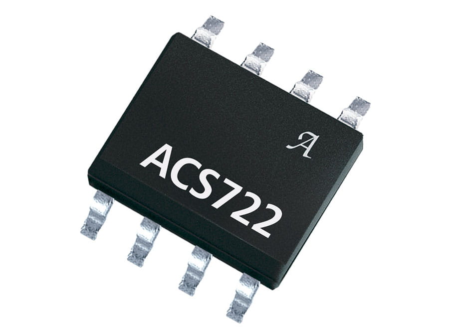
The ACS722 is provided in a small, low profile surface mount SOIC8 package or the higher isolation surface mount SOIC16W wide body package. The leadframe is plated with 100% matte tin, which is compatible with standard lead (Pb) free printed circuit board assembly processes. Internally, the device is Pb-free, except for flip-chip high-temperature Pb-based solder balls, currently exempt from RoHS. The device is fully calibrated prior to shipment from the factory.

  • Patented integrated digital temperature compensation circuitry allows for near closed loop accuracy over temperature in an open loop sensor
  • UL60950-1 (ed. 2) certified
    • Dielectric Strength Voltage
      • ACS722LLC: 2.4 kVrms
      • ACS722KMA: 4.8 kVrms
    • Basic Isolation Working Voltage
      • ACS722LLC: 420 Vpk or VDC / 297 Vrms
      • ACS722KMA: 1550 Vpk / 1097 Vrms or VDC
    • Reinforced Isolation Working Voltage
      • ACS722KMA: 800 Vpk / 565 Vrms or VDC
  • Industry-leading noise performance with greatly improved bandwidth through proprietary amplifier and filter design techniques
  • Pin-selectable band width: 80 kHz for high bandwidth applications or 20 kHz for low noise performance.
  • Primary conductor resistance for low power loss and high inrush current withstand capability
    • ACS722LLC: 0.65 mΩ
    • ACS722KMA: 0.85 mΩ
  • Packages:
    • ACS722LLC: Small footprint, low-profile SOIC8 package suitable for space-constrained applications
    • ACS722KMA: Low-profile SOIC16 wide-body package suitable for space-constrained, high isolation applications
  • ACS722LLC: Integrated shield virtually eliminates capacitive coupling from current conductor to die, greatly suppressing output noise due to high dv/dt transients
  • 3 to 3.6 V, single supply operation
  • Output voltage proportional to AC or DC current
  • Factory-trimmed sensitivity and quiescent output voltage for improved accuracy
  • Chopper stabilization results in extremely stable quiescent output voltage
  • Nearly zero magnetic hysteresis
  • Ratiometric output from supply voltage
ACS722 Current Sensor Integrated Circuit Packaging Image

The ACS722 is provided in a small, low profile surface mount SOIC8 package or the higher isolation surface mount SOIC16W wide body package. The leadframe is plated with 100% matte tin, which is compatible with standard lead (Pb) free printed circuit board assembly processes. Internally, the device is Pb-free, except for flip-chip high-temperature Pb-based solder balls, currently exempt from RoHS.

LC Package Documentation

MA Package Documentation

Part Number Specifications and Availability

Documentation and Resources

Documentation

Design Tools

Filter Document Type:
All Types
All Types FAQ Selection Guide
Documents Found: 32
Document Type Document Name
FAQ
Current Sensors FAQ
Selection Guide
Allegro Product Selection Guide
Filter Document Type:
All Types
All Types CB Certificate Certificates of Compliance Gerber File Simulation Tool SPICE Model
Documents Found: 32